On this page, after explaining the mechanism of bonding and the process of ultrasonic bonding, we will introduce how adwelds deals with ultrasonic bonding.
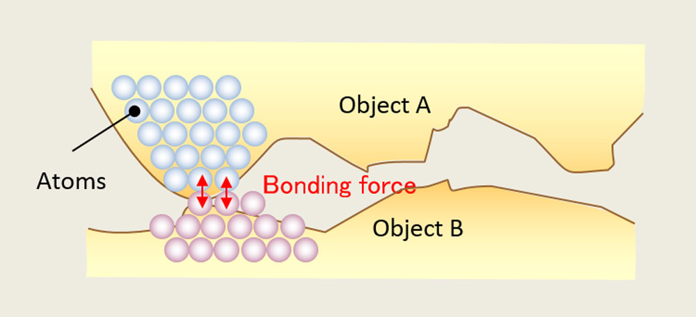
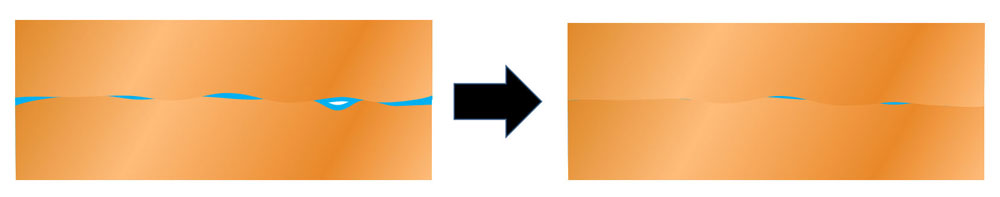
Ultrasonic reduces the metal objects to nearly an “interatomic spacing” level to bond
There are three ways to break down an object to the “interatomic spacing” level
Use the bonding power among atoms to bond the applications together
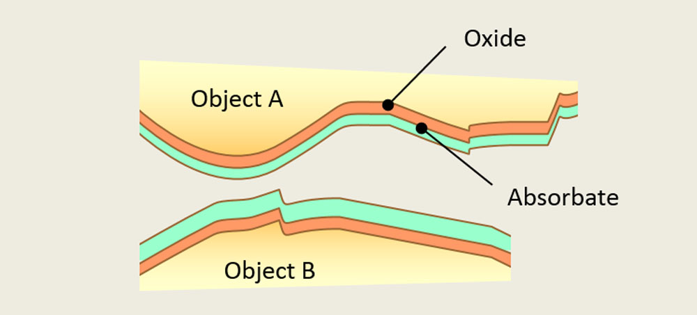
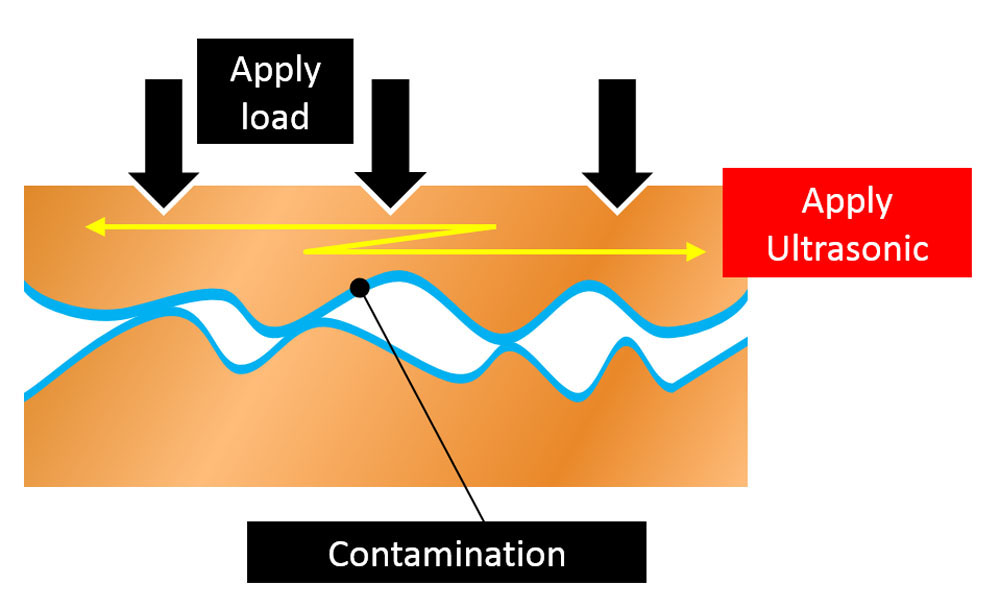
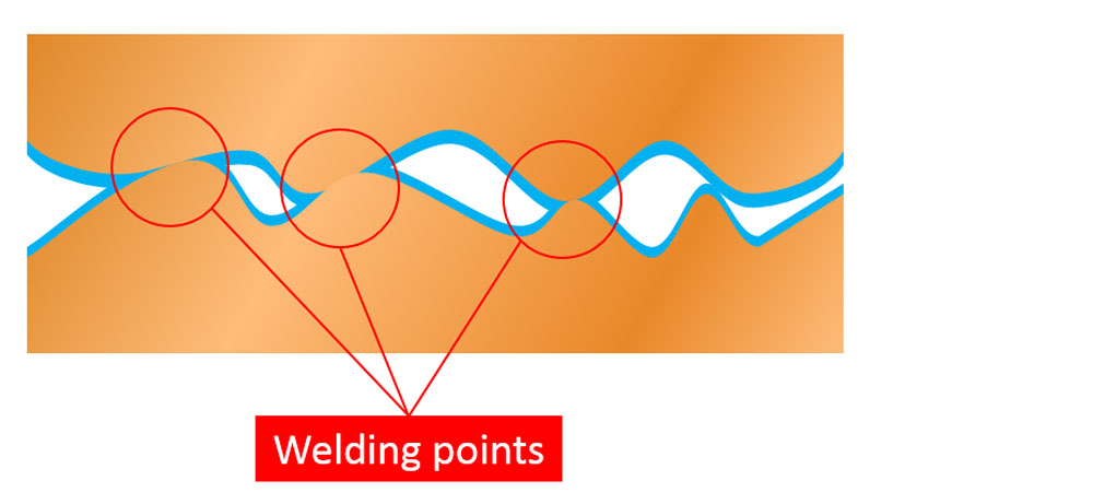
Obstructive factors listed below must be eliminated for bonding
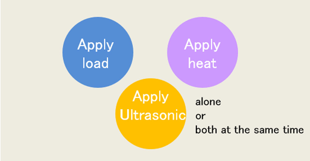
Usually, measures of applying ultrasonic or flux (when soldering) are taken to eliminate them
Diagrams below show ultrasonic processes how ultrasonic rigidly bonds applications without dissolving them.
This is a process developed together with Kyushu University an advanced ultrasonic technology, which bonds application at room temperature.
Fusion technology that consist of adwelds’ ultrasonic bonding technology and Kyushu University’s compliant micro bump technology.
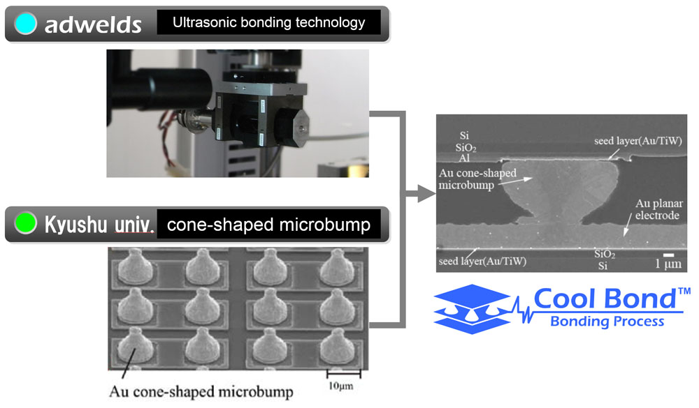
It can be useful in a 3D semiconductor or flexible electronics fields
adwelds developed a technology that bonds applications via a binder
Merit 1: Bond solderless Cu terminals on a printed circuit board
[Conventional Process]
When bonding Cu electrodes on the printed circuit board, it required soldering process. In order to increase reliability under high temperature, developing a technology of solderless direct bonding was on high demand. However, the ground of electrode is made of plastic resin that is soft; as shown in the diagram on the right, and damages were made on the Cu foil.
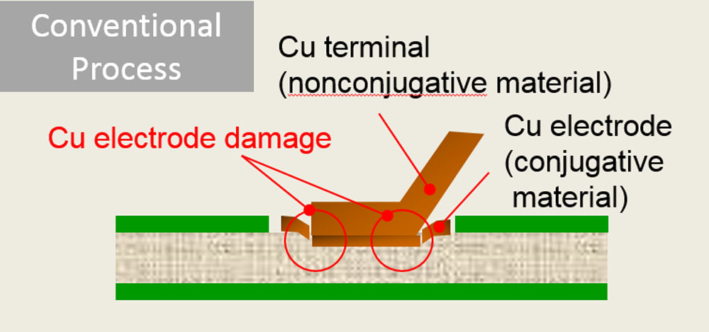
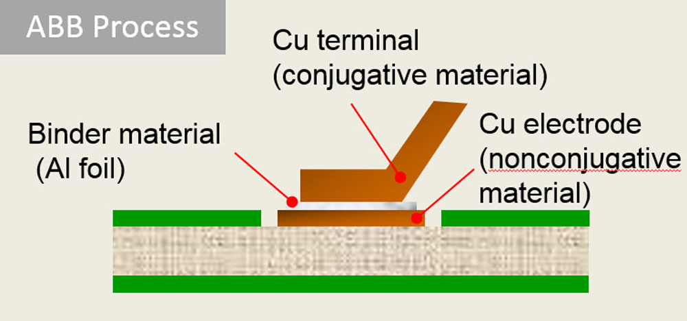
[ABB Process]
Adwelds developed a technology that bonds applications via a binder, a metal material that deforms easily such as Al. By using a metal binder, it stabilizes the bonding process without damaging electrodes on the printed circuit board.

[Conventional Process]
The conventional process put applications on top of each other, so the welding part gets thick. Applications that are difficult to weld when the welding part gets thick, needed to take measures.
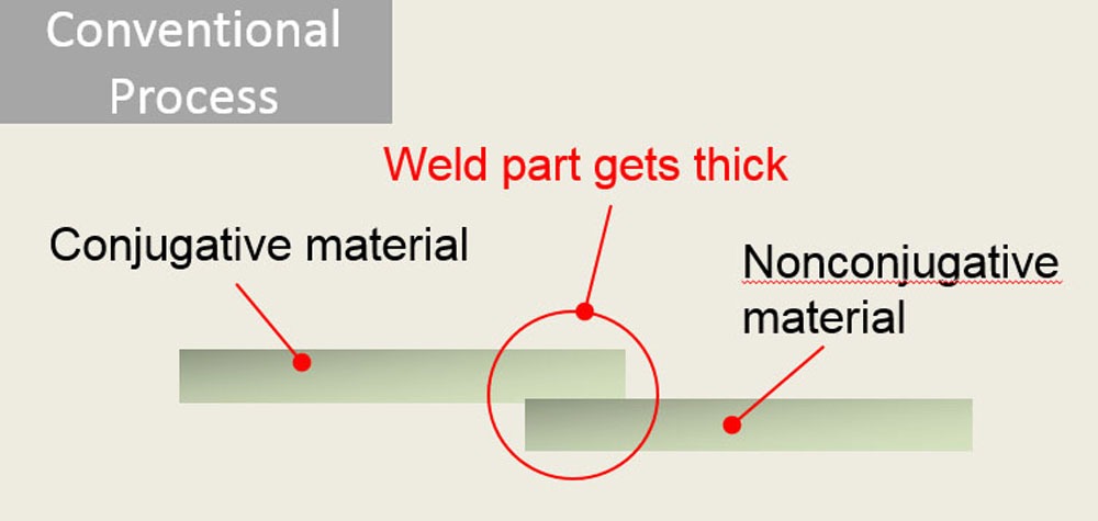
[ABB Process]
adwelds found a solution to this problem, the ABB Process: Place two applications as shown in the diagram and weld the binding materials; such as Al foils. The thickness of the welding part is the thickness of Al foils.